- 首页 >> Research >> Research Progress
Research Progress
Shanghai Institute of Technical Physics (SITP) and Fudan University make an important progress in the study of imaging nonlocal hot-electron energy dissipation
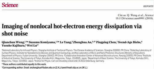
The group of Prof. Wei Lu in National Laboratory for Infrared Physics (SITP) and the group of Prof. Zhenghua An in Fudan University carried out a collaborating work that directly images the nanoscale nonlocal hot-electron energy dissipation via shot noise. The work titled “Imaging of nonlocal hot-electron energy dissipation via shot noise” (DOI: 10.1126/science.aam9991) has been published in Science (First release) on March 29th, 2018. The result is achieved because a novel near-field microscope called scanning noise microscope (SNoiM) has been developed based on a home-made ultrasensitive quantum well infrared detector.
The research results are online on Science (Preprint)
Since the discovery of electron for more than a century, human society becomes more and more relying on it. Nowadays electron has become the physical cornerstone of microelectronics and optoelectronics. As microelectronic devices continuously shrinking their sizes down to the nanoscale following the Moore’s Law, we face a great challenge in understanding the electron behavior which requires to develop a non-equilibrium theory from existing quasi-equilibrium theory. As pointed out in the report of the US Basic Energy Science Advisory Committee, one of the five major challenges we face in modern science is the characterization and control of far non-equilibrium state. Probing the non-equilibrium electron kinetics separately from the host crystal lattice are of great importance, leading to a better understanding and manipulation of hot electrons for future device applications.
According to the (quasi-) equilibrium theory, the electron temperature in a microelectronic device is highest at the position where the current density is the largest. But it is no longer true for nanoscale systems as pointed out in the paper: In nanoscale systems, the electrons can be much hotter than the host crystal lattice, and the highest electron temperature is not located at the position where the current density is the largest, but shifted to the downstream side of the electron flow. These interesting features have been confirmed both experimentally and theoretically, which arise from the non-equilibrium nature of hot electrons. We can simply analogy this novel feature of electron motion to the water flow. In a flat stream, the water is in quasi-equilibrium, and the slowly flowing water follows the topography of the riverbed landform with a noise-less feature. Once it passes through the landform with a sudden drop, the water is accelerated and hits the trough of the river bed, generating large fluctuations. In this case, the water flow is no longer completely attached to the tomography. Just like the boiled water heated to a high temperature, if we use an effect temperature to describe the water here, the temperature should be very high so that it can generate such a large fluctuation. Similarly, by applying a source-drain voltage to a nanoscale device, the electrons are accelerated by a large electric field and dissipate their excess energy in the drain side, causing large current fluctuations. The estimated effective electron temperature is much higher than that of the crystal lattice.
Experimentally, it is extremely challenging to directly image the hot electron dynamics. In this paper, a sensitive infrared near-field microscope, called scanning noise microscope has been developed and applied. The detection mechanism is that: Non-equilibrium electrons accelerated by the electric-field cause large current fluctuations, which generates fluctuating electromagnetic (EM) evanescent fields at the sample surface. The fluctuating EM evanescent fields are then scattered by a nanoscale tip and the scattered radiation is sensitively detected by a home-made infrared detector. Electron temperature instead of lattice temperature is exclusively probed because the evanescent fields are mainly generated by the non-equilibrium electrons. The developed SNoiM provides a very unique experimental tool for investigating non-equilibrium electrons in nanoscale systems.
More innovative results will be achieved in National Laboratory for Infrared Physics with the publication of this paper. This work was supported by National Natural Science Foundation, National Key Research Program of China, Shanghai Science and Technolog Committee and Chinese Academy of Sciences Visiting Professorships for Senior International Scientists.
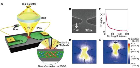
Fig. 1. Nanoscale mapping of ultrahigh-frequency excess noise (21.3 ± 0.7 THz) with scanning noise microscope (SNoiM). (A) Schematic representation of the experimental setup of SNoiM [section 1 of (27)]. (B) SEM image of the nanodevice with a constriction fabricated in a GaAs/AlGaAs quantum well (QW) structure. (C and D) Two-dimensional real-space images of the NF signal intensity (excess noise), for opposite bias polarities (±6 V). The horizontal and vertical scales are those of the SEM image of (B). The NF signals are taken by modulating the tip height. The color scale is given by the signal amplitude V (detector output) as well as by the effective electron temperature Te (K). The electric field at the constriction is estimated to be Ec ≈ 62 kV/cm for Vb =6.0 V. (E) Decay profile of the NF signal with increasing the tip-height h from 5 nm to 150 nm, taken at the center of constriction with Vb = 6 V. The signal is obtained by modulating Vb between 0 and 6 V without modulating the tip height
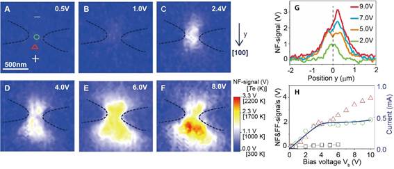
Fig. 2. Evolution of the excess noise distribution with increasing bias voltage, Vb. (A to F) Two-dimensional images obtained by modulating the tip height. The crystallographic orientation is y//[100]. (G) One-dimensional profile of the NF signal intensity in the y direction, where y = 0 corresponds to the center point of the constriction marked by the green circle in Fig. 2A. The data are taken by modulating Vb.(H) The solid line shows the current versus Vb curve. Green circles and red triangles show, respectively, the NF signals (excess noise intensities) at the positions marked by o (y =0) and D (y = +250 nm) in Fig. 2A. The data are taken by modulating Vb. The black squares plot the FF signal, obtained by modulating Vb without using the tip, showing that the current-induced FF component is less than a few percent of the NF signal.