- 首页 >> Research >> Research Progress
Research Progress
Progress in the study of doping low-dimensional materials by ferroelectric field
A small optoelectronic/electronic component that has caused one of the most dramatic outpourings of technological progress in human history. With the development of semiconductor technics, further requirements are put forward for material properties and device structure. With the emergence of low-dimensional materials in recent years, its unique structure and physical properties have attracted much attention, and it has shown its potential in electronic and optoelectronic devices. The physical basis of semiconductor functional devices is to control the type and concentration of carriers by elemental doping. As to the low-dimensional semiconductor materials, how to realize the precise control of its carriers is also the only way to fabricate functional devices.
Recently, researchers from Shanghai Institute of Technology Physics (CAS), in collaboration with research groups from Fudan University, Nanjing University, East China Normal University, and Institute of Microelectronics, put forward a new method of doping low-dimensional semiconductor materials by using non-volatile ferroelectric polarization field and fabricate a variety of novel electronic and optoelectronic devices based on this method.
Specifically, researchers proposed two methods to construct low-dimensional semiconductor optoelectronic devices by the ferroelectric polarization field. Firstly, the low-dimensional semiconductor is tuned by the ferroelectric field which is polarized by the nano-probe (“top-down approach”, Figure 1). When the positive/negative voltage is applied to the scanning probe, the ferroelectric polarization is downward/upward, and electrons/holes are injected into the semiconductor material. The feature of this method is that the device pattern can be edited arbitrarily, erased and rewritten, and the spatial size of the doping region can be defined accurately. Based on this method, researchers have constructed p-n junction, BJT transistor, and novel memory devices. Besides, a split-gate structure is constructed to polarize the ferroelectric thin film by applying a voltage to the solid-state electrode, so as to dope the low-dimensional semiconductor (“bottom-up” processing Figure 2). This method is characterized by solid-state structure, sufficient polarization, better electrical performance, and stability. The p-n junction photodetectors and photovoltaic devices can be realized by using the above two methods, whose response range extends up to the SWIR at room temperature.
The above two methods of doping low-dimensional semiconductors by the ferroelectric polarization field provide a new technical way for the functional application of low-dimensional semiconductors. Relevant research results have been published in Nature Electronics (doi.org/10.1038/s41928-019-0350-y) and Advanced Materials (doi.org/10.1002/adma.201907937)
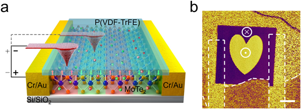
Figure 1. Low-dimensional semiconductor homojunctions controlled by probe-polarized ferroelectric domains.
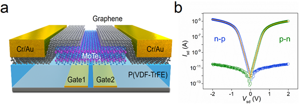
Figure 2. Solid-state structure of low-dimensional semiconductor p-n junction controlled by ferroelectric polarization.