- 首页 >> Research >> Research Progress
Research Progress
Functionalizing van der Waal materials by shaping them
Recently, the researchers of the Shanghai Institute of Technical Physics, Chinese Academy of Sciences (Lu Wei, Li Tianxin, and Hu Weida) show an innovative way to fabricate two-dimensional PN junction. Such strategy greatly simplifies the semiconductor manufacturing process and is well-suited to develop (opto-)electronic devices at the ultimate physical limit. The related results were published online in the journal "Light: Science & Applications" on June 6 with the title of "Pristine PN junction toward atomic layer devices".
The study shows a striking fact that a number of two-dimensional layered materials don’t need artificial doping, they are doping themselves from n- to p- type conductance with an increasing/decreasing thickness (MoTe2, MoS2, WSe2, and BP). For example,MoTe2 material exhibits p-type, unintentional doping and n-type doping behaviors when it has one molecular layer, three molecular layers, and five molecular layer thickness, respectively. Using this novel property, researchers can easily fabricate atomically abrupt PN junctions on a variety of two-dimensional materials, which is out of the range of traditional technique (Figure 1).
As shown in Figure 2, there are no complicated photolithography and chemical doping processes in layered junction devices. Instead, people has only needed to shape the geometry of the material.
Just as stated in the paper “Findings disclosed here might open up a path to develop novel nanodevice applications, where the geometrical size becomes the only critical factor in tuning charge-carrier distribution and thus functionality.”
Xia Hui (Associate professor) is the first author, and Lu Wei, Li Tianxin, and Hu Weida (professors) are the corresponding authors of the paper. The research was supported by the National Natural Science Foundation of China and the Shanghai Natural Science Foundation.
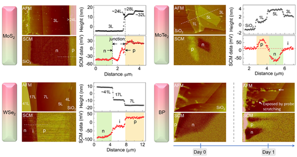
Figure 1. Self-doping behavior of the two-dimensional materials
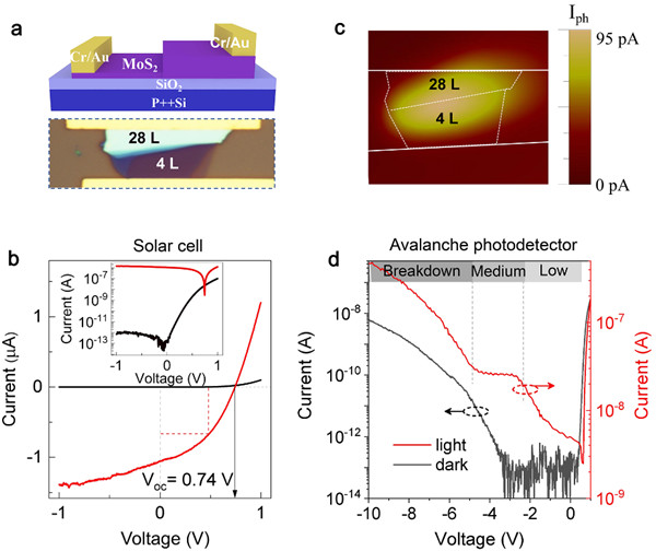
Figure 2. Layer PN junction and diode device based on it. a, device structure, b, scanning photocurrent image, c, photovoltaic IV curve, d, avalanche photodetector
Original link:https://www.nature.com/articles/s41377-022-00814-8