As a high-k material, SrTiO3 (STO) has attracted much attention because it can be used as an alternative material to replace the conventional SiO2 for further development of CMOS devices. In addition, due to its lattice closely matching to both silicon substrate and most of the crystalline oxides, STO/Si system can also be used as one kind of pseudosubstrate for fabricating the Si-based crystalline oxide functional devices, such as smart card, surface acoustic wave (SAW) filters, optical modulators, nonvolatile ferroelectric random access memory (NVFRAM), and so on.
In general, an amorphous interfacial layer was always inevitably formed at the STO/Si interface due to the intrinsic thermaldynamic instability between STO and Si during the standard growth process. It has been pointed out that the existence of such an interfacial layer is an advantage to some extent. This interfacial layer can enlarge the band offset between STO and Si, and consequently improve the leakage property. Up to now, there is a tremendous interest in the study of the STO/Si interface. Nowadays, many studies have transferred the research emphasis from how to eliminate the STO/Si interfacial layer as much as possible by using some special methods, to how to optimize and employ this interfacial layer to obtain good performance of devices, which was called as interface engineering. In the actual devices, the intrinsic STO layer and the STO/Si interfacial layer are in series. When applied a gate voltage, it is expected that there must exist a tolerable divided-voltage applied onto the interfacial layer, excess that charges can be injected into the interfacial layer. Such a charge injection behavior will enlarge the leakage current, and consequently affect the reliability of devices.
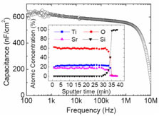
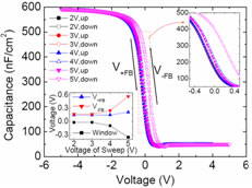
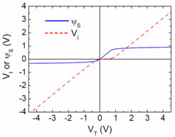
Highly (h00) preferential oriented SrTiO3 (STO) thin films were grown on p-Si(100) substrates by RF magnetron sputtering technique by our group. The electrical properties of the STO/Si interfacial layer were studied by measuring MIS structures. A low-k interfacial layer composed of Si, O, Sr and Ti atoms was formed at the STO/Si interface during the growth process of STO (AES of Fig.1). The capacitance-voltage (C-V) characteristic with different sweep voltages was measured for STO MIS structures (Fig.2). Under the higher sweep voltages, the C-V characteristic curves of STO MIS structures showed counterclockwise loop behaviors. As the sweep voltages further increasing, the window of the counterclockwise C-V loops increased accompanying the flat band voltages for both the up and the down sweeps mono-shifting towards the positive direction. It was considered that such counterclockwise loop behaviors were associated with the electron injection at the STO/Si interface. The electrons were injected from the semiconductor Si substrate into the interfacial layer through the STO/Si interface under the positive electric filed. In addition, the voltage distribution of the semiconductor Si, the insulator STO, and the STO/Si interfacial layer in the STO MIS structure was analyzed in details (Fig.3). The electric field applied onto the interfacial layer leading to the onset of the electron injection (named as the electron injection electric field of interfacial layer) was calculated to be about 5.5MV/cm.
For further development of Si-based integrated devices, the high-k materials will act as more and more important roles. It should be pointed out that other high-k materials, such as Gd2O3, CaZrOx, HfO2, ZrO2, TiO2, Ta2O5, PbTiO3, PbZrO3, SrBi2Ta2O9, and so on, similar to STO, also inevitably faced with such an interface problem when directly grown on Si substrates. Moreover, compared with the conventional SiO2 gate material, the band gaps of these high-k materials are relatively narrow and the band offset between high-k materials and Si is also relatively small, which suggests that these high-k/Si interfaces should also be optimized. Therefore, the analysis process and the results obtained in the present work are not just proper for the STO/Si system, and can also provide some valuable instructions for the design and the preparation of the Si-based integrated devices with other high-k materials.
This work has been published in Applied Physics Letters [J.H. Ma, J.L. Sun, J.H. Qin, Y.H. Gao, T. Lin, H. Shen, F.W. Shi, X.J. Meng, J.H. Chu, S.J. Liu, J. Li, “Electron injection of SrTiO3/Si interfacial layer”, Applied Physics Letters, 2008, 93: 102903].

Fig.1 C-F characteristic curve of STO MIS structure. The inset shows AES depth profile of STO/Si.

Fig.2 C-V plots of STO MIS structure under different sweep voltages. The inset shows the evolution of the flat band voltages and the loop windows for different C-V sweeps.

Fig.3 Relationship among the total gate voltage (VT), insulator voltage (VI) and semiconductor surface potential (yS) for ideal MIS.
|